Description of the image

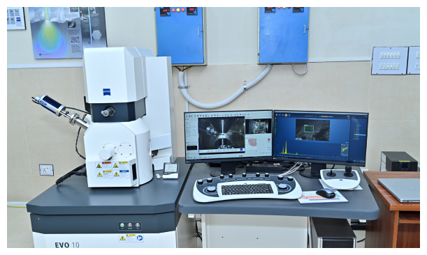
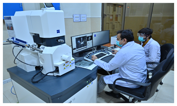
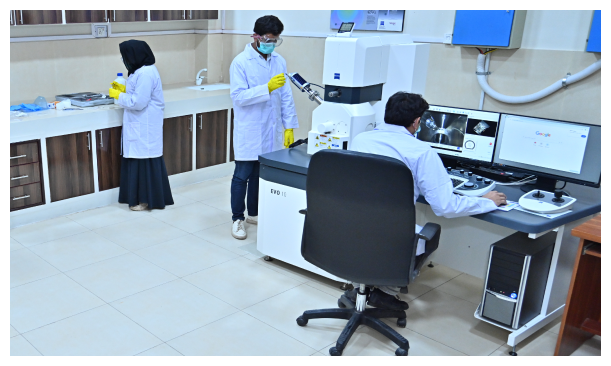
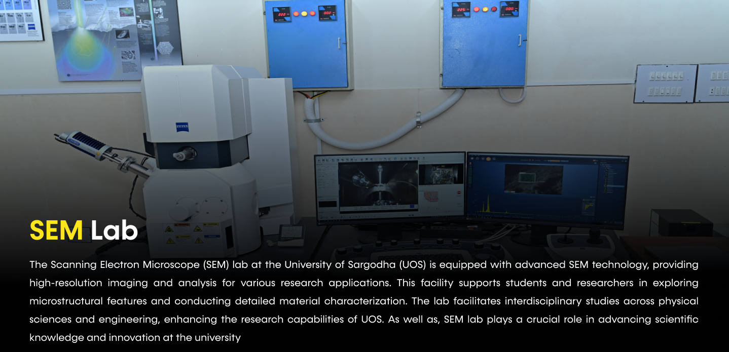
Scanning Electronic Microscope

The Scanning Electron Microscope (SEM) is a powerful tool that uses focused beams of high-energy electrons to scan the surface of samples, producing detailed, high-resolution images and providing valuable surface information. Its ability to create three-dimensional images and analyze microstructures makes it indispensable in various scientific fields, including materials science, biology, and nanotechnology.

Image 1
Image 2
Image 1
Image 2

SEM follows precise steps, benefiting student research

Image 1
Electron Beam Generation

An electron gun produces a focused beam of high-energy electrons.

Image 1
Sample Interaction

The electron beam is directed onto the surface of the sample, causing interactions with the sample's atoms.

Image 1
Signal Emission

Various signals (secondary electrons, backscattered electrons, and X-rays) are emitted from the sample as the electron beam interacts with it.

Image 1
Detection

Detectors capture these signals to form high-resolution images, displaying the sample's surface features in detail.

Image 1
Image Formation

The emitted signals are processed to create a magnified image of the sample, allowing analysis at the nanometer scale.

Gold Au-sputter

A Gold (Au) Sputter Machine is a device used in materials science and surface engineering for the deposition of thin films of gold onto various substrates. This process is crucial for enhancing the properties of materials and enabling advanced imaging techniques in electron microscopy.

Image 1

Discover Insights from Leading Voices

What Our Experts Say About the One Health Approach

Experts share valuable perspectives on the One Health approach, highlighting its significance in fostering a healthier, interconnected world.

Learn More